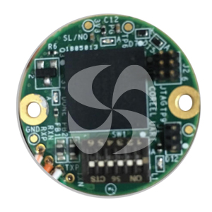
SigmaDelta Analog to Digital Convertor (SDADC)
SDADC is an integrated design of two PCBs, the first PCB (Signal conditioning board)has pre-amplifier, anti-aliasing filter, programmable gain array(digital potentiometer) and Sigma Delta ADC and the second PCB(Digital board)has Intel Max 10 FPGA which is stacked with the first PCB acts as a controller for the functioning of both the PCBs.
Digital Board receives ADC data and convert it to suitable frame format using the Intel Max 10 FPGA. FPGA alsogenerates clock signal for the ADC and controls the SPI mode of operation of the ADC. Gain control bits for the digital potentiometer arealso controlled by FPGA.
Key Features
- Circular form factor with 25 mm diameter.
- Low noise pre-amplifier stage from 10 Hz to 4 KHz with 40 dB gain
- Programmable gain from 0 dB to 40 dB via digital potentiometer
- 24-bit delta-sigma ADC with a data rate up to 105kSPS
- Intel FPGA Max 10
- Transmit serial data over RS485 interface on receiving command over RS485 interface.
